In the realm of computer chips,phim khiêu dam au m? nam 80 bigger numbers are often better. Morecores, higherGHz, and greaterFLOPs, are all desired by engineers and users alike. However, there's one metric in semiconductors that keeps gaining attention and relevance: the smaller, the better. Welcome to the world of semiconductor manufacturing and the technology node, also known as the process node.
But what exactly is it, and why does it hold such significance? Why is it measured in nanometers, and why are the numbers 10, 7, and 5 prominently featured in this article? Let's take a journey into the world of process nodes...
Before we proceed, you may want to go through our series of CPU architecture features to gain a better understanding of things. In the first part, we cover the basics of how processors work and in part two, we explore the planning and design of chips.
The key section relevant to this article is the one detailing how computer chips are physically put together. You'll want to read the section on photolithography carefully if you want an in-depth understanding of the manufacturing process, while in this article we'll focus more on this point that was briefly touched upon:
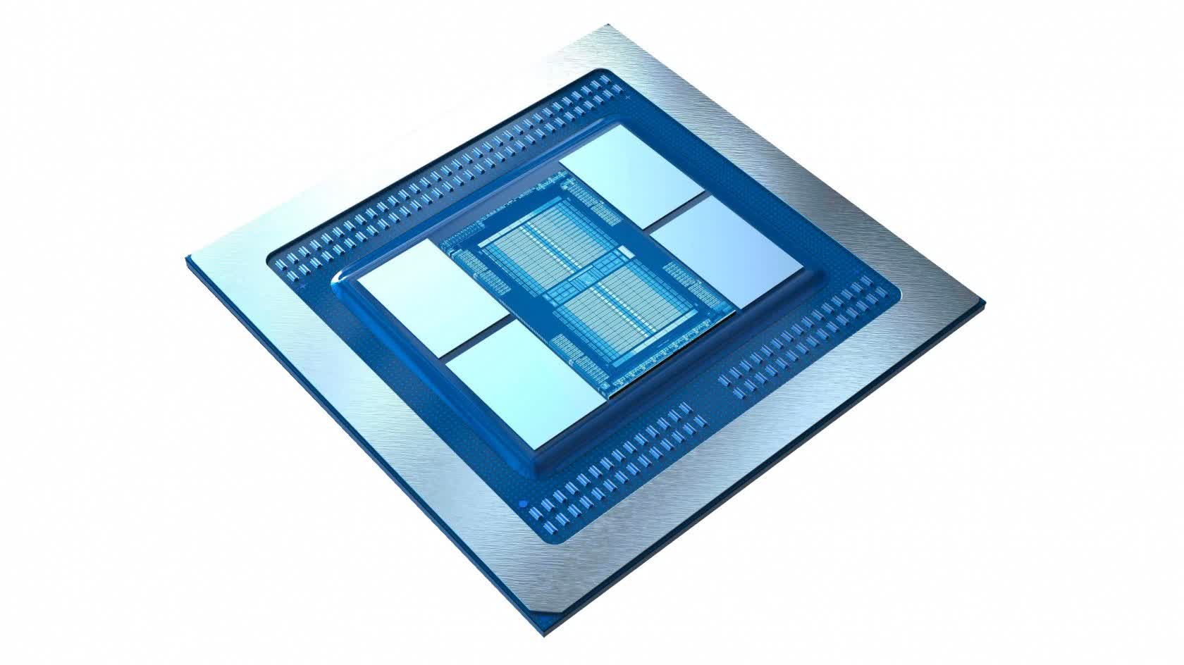
One of the biggest marketing terms associated with chip fabrication is the feature size.
In the chip industry, the term "feature size" is associated with the process node. As discussed in "How CPUs are Designed, Part 3," the term is somewhat flexible. Different manufacturers use it to describe varying aspects of the chip. Not so long ago, it specifically denoted the smallest gap between two sections of a transistor.
These days, it's more of a marketing term and not very useful for comparing production methods. Nonetheless, the transistor is a critical feature of any processor, as groups of them perform all of the number crunching and data storage done inside the chip, and a smaller process node from the same manufacturer is highly coveted. Why, you might ask?
No activity in the processor world happens instantaneously, and every operation demands electrical energy. Larger components take more time to change states. Signals require more time to traverse, and it takes more energy to circulate electricity within the processor. Put simply, larger components occupy more physical space, making the chips themselves bulkier.
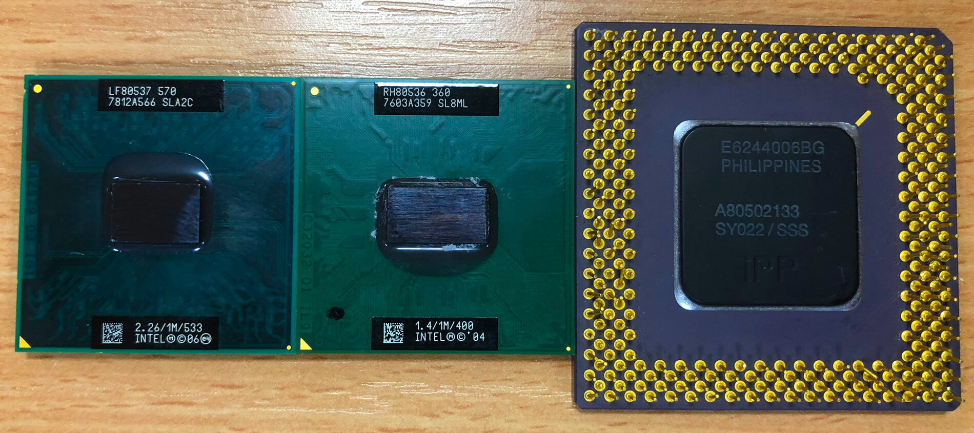
In the above image, we observe three vintage Intel CPUs. From left to right: a 2006 Celeron, a 2004 Pentium M, and an older Pentium from 1995. Their process nodes are 65nm, 90nm, and 350nm, respectively. To put it another way, the critical parts in the 28-year-old design are over five times larger than those in the 17-year-old model. Another noteworthy distinction: the newer chip houses approximately 290 million transistors, while the original Pentium boasts just over 3 million - nearly a hundred times fewer.
While the reduction in process node contributes to the recent design's smaller physical size and its higher transistor count, it undeniably plays a pivotal role in Intel's advancements.
But here's the real kicker: that Celeron generates approximately 30W of heat, whereas the Pentium emits a mere 12W. This heat emanates primarily from the movement of electricity through the chip's circuits. As electricity flows, energy dissipates due to various processes, with the vast majority being released as heat. While 30 is certainly higher than 12, it's vital to remember that the Celeron boasts nearly 100 times more transistors.
Given that a smaller process node offers the advantages of more compact chips packed with more transistors that can toggle more swiftly – translating to a higher number of calculations per second – and lesser energy released as heat, it naturally raises a question: Why isn't every chip in the world manufactured using the smallest possible process node?
Let there be light!
At this point, it's essential to understand a process called photolithography. Here, light passes through a device known as a photomask, which obstructs light in certain areas and allows it to penetrate in others. Where the light passes through, it's intensely concentrated into a small area. This light then interacts with a special layer used in chip manufacturing, delineating the positions of the chip's various components.
Consider it analogous to an X-ray of your hand: the bones block the rays, acting like the photomask, while the flesh allows the rays to pass, resulting in an image that showcases the hand's internal structure.
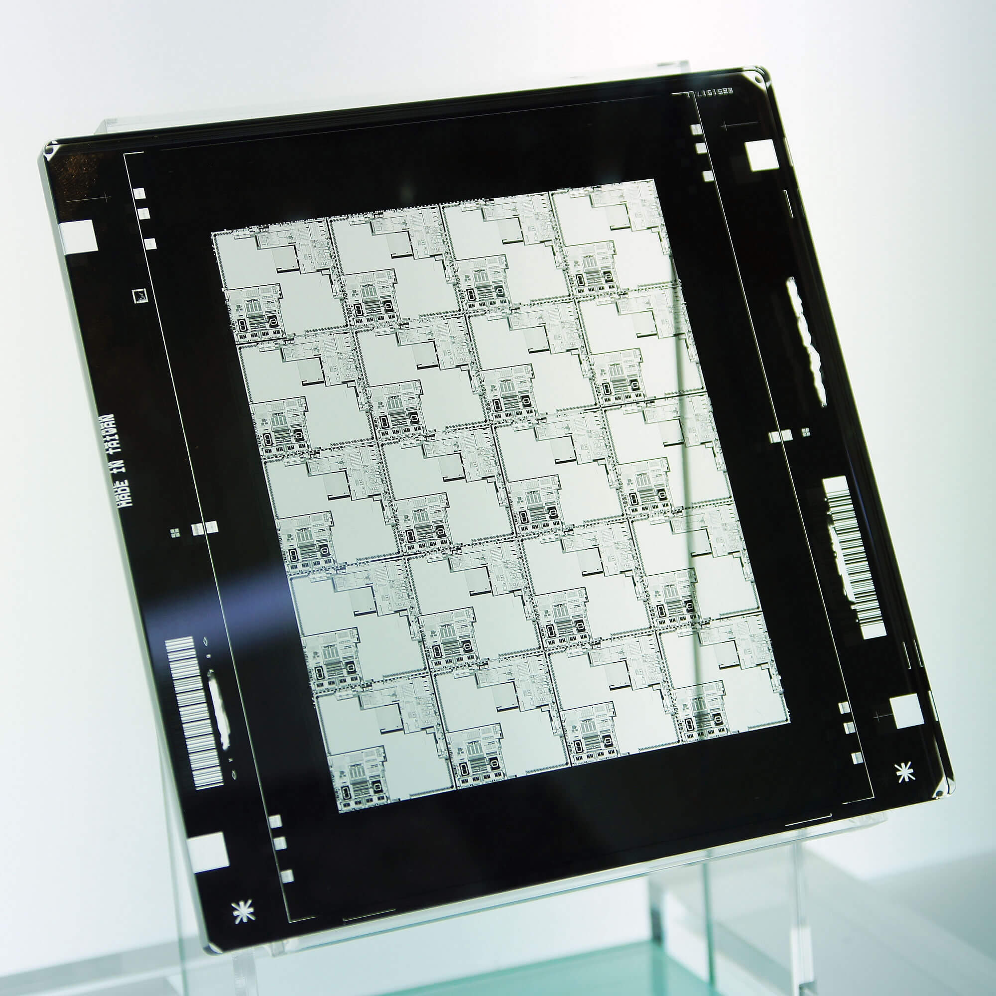
Image: Peellden, Wikimedia Commons
Interestingly, actual light isn't employed in this process. Even for older chips like the Pentium, light's "size" or wavelength is too large. Now, you might be wondering how on Earth light can have any size, but this is in reference to wavelength. Light is an electromagnetic wave, a perpetually oscillating fusion of electric and magnetic fields.
While we often represent it with a classic sine wave to visualize its form, electromagnetic waves don't truly have a distinct shape. Rather, the effects they produce upon interaction adhere to this sine wave pattern. The wavelength of this oscillatory pattern denotes the physical distance between two congruent points on the wave.
Imagine ocean waves lapping at a shore; the wavelength is the distance between consecutive wave crests. Electromagnetic waves exhibit a vast array of possible wavelengths, so we group them under the umbrella term "spectrum."
Small, smaller, smallest
In the image below, what we recognize as light is just a minuscule portion of the entire spectrum. This spectrum includes other familiar entities such as radio waves, microwaves, x-rays, and more.
Within this spectrum, light has wavelengths approximately around 10-7meters in size or roughly 0.000004 inches!
For such minute measurements, scientists and engineers favor using nanometers, or "nm" for short. If we delve deeper into a section of the spectrum, we observe that visible light actually spans from 380 nm to 750 nm.
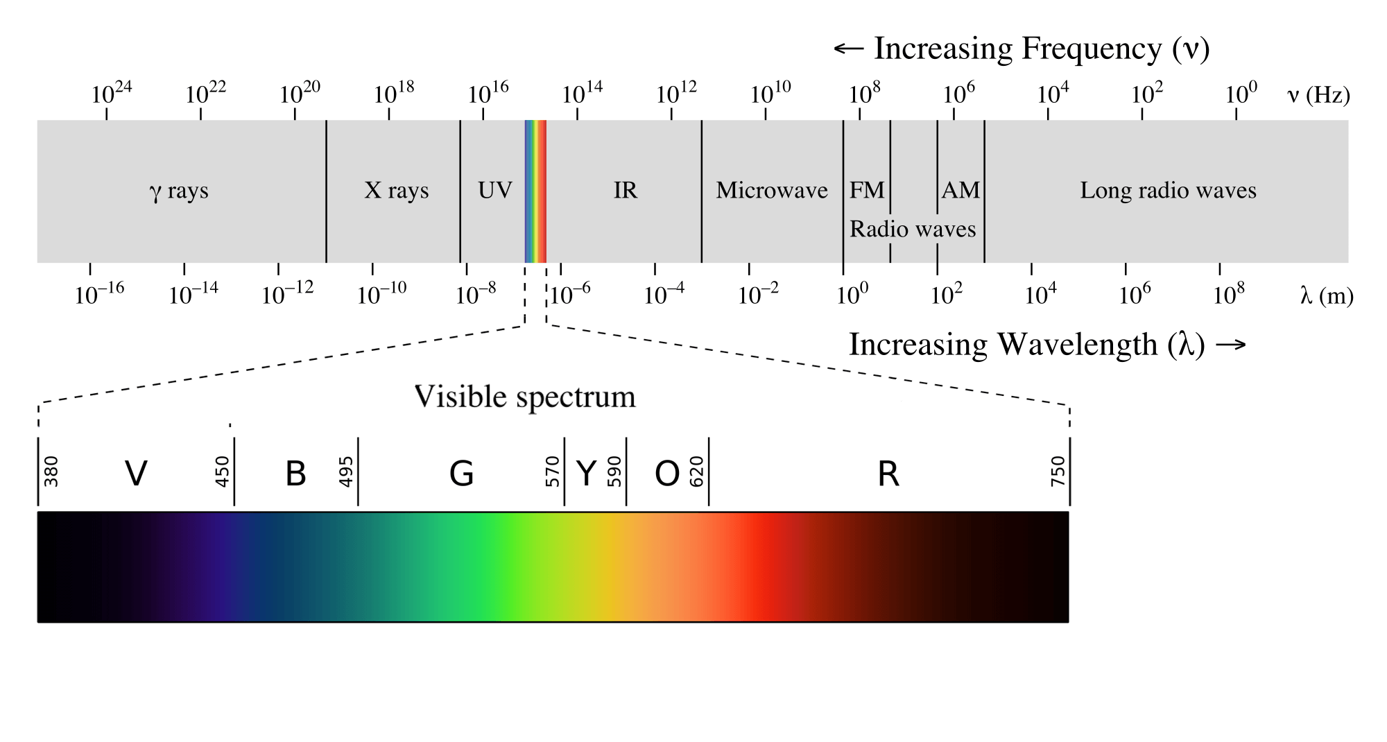
Image: Philip Ronan, Gringer
Recall the earlier mention of the old Celeron chip in this article – it was fabricated using a 65 nm process node. You might wonder, how can components smaller than visible light be created? Simple: the photolithography process didn't use light, it used ultraviolet light (a.k.a. UV).
According to the spectrum chart, UV begins at approximately 380 nm (where visible light culminates) and shrinks down to roughly 10 nm. Manufacturers like Intel, TSMC, and GlobalFoundries utilize an electromagnetic wave termed EUV (extremeUV), which is around 190 nm in wavelength. These shorter wavelengths not only permit the production of tinier components but also potentially enhance their overall quality. This allows the various parts to be packed in closer together, helping to scale down the overall size of the chip.
Different manufacturers assign distinct names to the scale of the process node they employ. Intel used a catchy name for one of their 10nm nodes: P1274, but they often represent it as "10 nm" for the lay audience. In contrast, TSMC simply labels theirs as "10FF."
Processor design firms like AMD create the layouts and structures suitable for these smaller process nodes, then rely on manufacturing giants like TSMC for production.
TSMC has been diligently advancing with ever-smaller nodes (7nm, 5nm, 3nm), crafting chips for major clients such as Apple, MediaTek, Qualcomm, Nvidia, and AMD. In this realm of manufacturing, some of the tiniest features measure just 6 nm across (though many features are substantially larger).
To grasp the sheer minuteness of 6 nm, consider this: the silicon atoms, which constitute the majority of a processor, are spaced about 0.5 nm apart, with each atom being approximately 0.1 nm in diameter. Hence, as a rough estimate, TSMC's facilities handle transistor elements that span fewer than 10 silicon atoms in width.
The challenge in aiming for atoms
Setting aside the mind-boggling reality that chip manufacturers are working towards features that span just a few atoms, EUV photolithography has raised a whole bunch of serious engineering and manufacturing challenges.
Intel faced considerable challenges in matching its 10 nm production to the efficiency of its 14 nm process, and GlobalFoundries encountered its own set of problems in scaling down to 7 nm and even smaller. While the complications faced by Intel and GlobalFoundries might not solely stem from the intricacies of EUV photolithography, it's unlikely that the two are entirely unrelated.
The shorter the wavelength of an electromagnetic wave, the more energy it embodies. This higher energy level poses a risk of causing damage during the chip manufacturing process. Ultra-precise fabrication is acutely susceptible to contamination and defects in the utilized materials. Furthermore, factors like diffraction limits and statistical noise – the innate variance in the location where energy from the EUV wave is deposited onto the chip layer – hinder the aspiration of producing flawless chips.
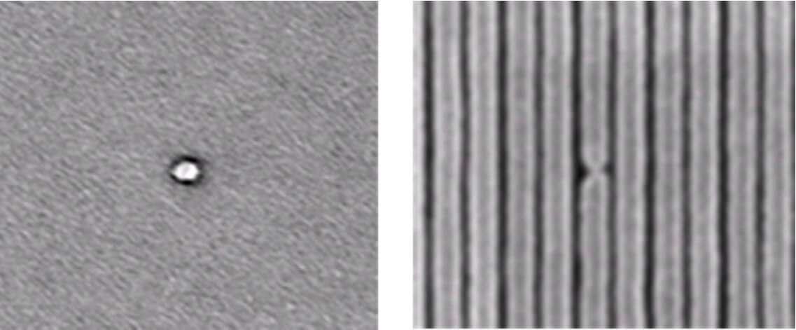
Two manufacturing defects in a chip. Image: Solid State Technology
At the atomic level, traditional understandings of electricity and energy transfer no longer hold firm. Ensuring the flow of electricity – in the form of moving electrons, one of the three subatomic particles – through closely placed conductors is fairly straightforward at familiar scales; one can simply encase the conductors in a robust insulating layer.
However, at the scales where Intel and TSMC operate, this task becomes daunting, primarily because the insulation isn't sufficiently thick. Yet, for now, most production challenges can be attributed to the complexities intrinsic to EUV photolithography. Thus, we might have to wait a few more years before we dive into senseless debates on forums about Nvidia's edge over AMD in handling quantum behavior – or vice versa.
This is because the real problem, the ultimate reason behind the production difficulties, is that Intel, TSMC and all their fabricating chums are businesses, and they're aiming for atoms for the sole purpose of generating future revenue. In a research paper by Mentor, the following overview was offered as to how much more wafers cost for smaller process nodes...
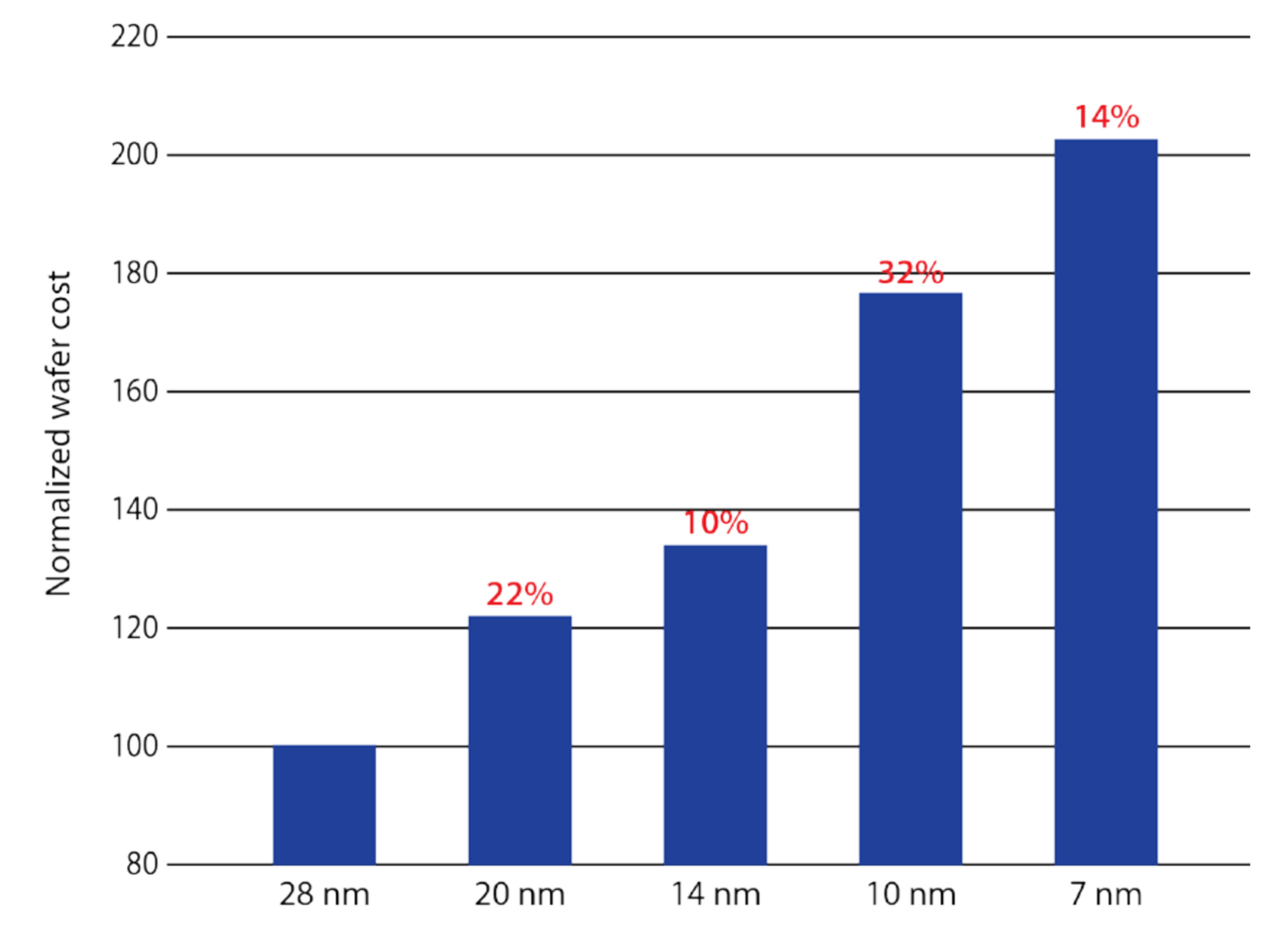
Let's assume that Intel's 28 nm process node was employed for their Haswell CPU series (e.g., the Core i7-4790K). If so, their 10 nm approach costs nearly double per wafer. While the number of chips a wafer can yield largely hinges on chip size, smaller process nodes might allow for a greater chip yield per wafer, somewhat offsetting the rise in costs. Ultimately, manufacturers will attempt to transfer as much of this cost to consumers via price hikes. However, they must strike a balance considering market demand.
The surge in smartphone sales (and the SoCs powering them) in the last decade, along with a near exponential growth in smart technology in homes and cars, has meant that chip manufacturers have been forced to absorb the financial hit from going to smaller process nodes until the whole system is mature enough to churn out high yielding wafers.
This will continue until their systems mature enough to consistently produce high-yield wafers – those with minimal defects – in bulk.
Given the stakes are in the realm of billions of dollars, it's a precarious endeavor. This kind of financial gamble was part of the reason why GlobalFoundries bailed out of the process node race.
Future prospects
If this all sounds somewhat doom-and-gloom, it's essential to remember that the immediate future is promising. Samsung and TSMC have successfully operated their 7 nm production lines for some time now, delivering impressive volume and revenue. Moreover, chip designers are future-proofing their designs by utilizing multiple nodes in their products.
AMD's chiplet design strategy with Ryzen CPUs has set a precedent for other chip makers. For example, their 3rd-gen Ryzen CPUs that debuted back in 2019, incorporated two chips made on TSMC's 7 nm node and one 14 nm chip crafted by GlobalFoundries. The former were the actual processor parts, while the latter managed DDR4 memory and PCI Express devices connected to the CPU.
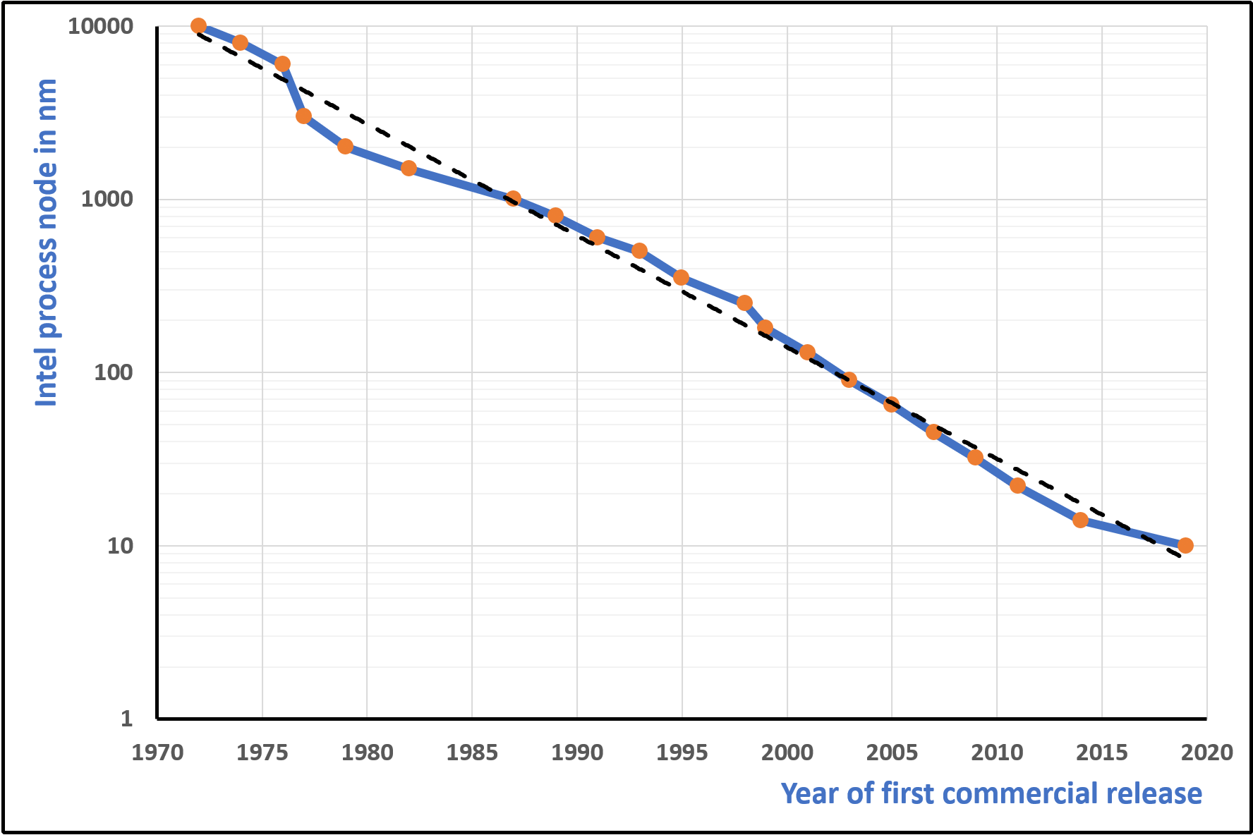
The chart above illustrates Intel's process node evolution over the past 50 years. On the vertical axis, the node size is showcased in factors of 10, starting all the way up at 10 000 nm. The chip giant's trajectory suggests a rough node half-life (the time taken to reduce the node size by half each time) of 4.5 years.
Does this trajectory indicate an Intel 3 nm - 5 nm release by 2025? It's highly likely. Even with previous hiccups, Intel's recovery efforts are in full swing. Meanwhile, Samsung and TSMC are already progressing with their 3 nm production and further innovations. The outlook is indeed optimistic for processors across the spectrum.
These future processors promise to be more compact and efficient, consuming less power while delivering superior performance. They pave the way for advancements like fully autonomous vehicles, smartwatches that rival the power and battery longevity of contemporary phones, and gaming graphics (or should we say AI chips?) that surpass the visual marvels of blockbuster films from a decade ago.
The future is bright indeed, because the future is small.
Keep Reading. Explainers at TechSpot
- What Are Chiplets and the Future of Processors
- What is HDR?
- The Inner Workings of PCI Express
- Number Representations in Computer Hardware, Explained